- Like
- SHARE
- Digg
- Del
- Tumblr
- VKontakte
- Flattr
- Buffer
- Love This
- Save
- Odnoklassniki
- Meneame
- Blogger
- Amazon
- Yahoo Mail
- Gmail
- AOL
- Newsvine
- HackerNews
- Evernote
- MySpace
- Mail.ru
- Viadeo
- Line
- Comments
- Yummly
- SMS
- Viber
- Telegram
- JOIN
- Skype
- Facebook Messenger
- Kakao
- LiveJournal
- Yammer
- Edgar
- Fintel
- Mix
- Instapaper
- Copy Link
Production of chips using leading-edge process technologies requires more compute power than ever. To address requirements of 2nm nodes and beyond, NVIDIA is rolling out its cuLitho software library that uses the company’s DGX H100 systems based on H100 GPUs and promises to increase performance available to mask shops within a reasonable amount of consumed power by 40 times.
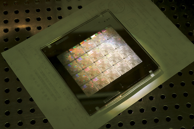
Modern process technologies push wafer fab equipment to its limits and often require finer resolution than is physically possible, which is where computational lithography comes into play. The primary purpose of computational lithography is to enhance the achievable resolution in photolithography processes without modifying the tools. To do so, CL employs algorithms that simulate the production process, incorporating crucial data from ASML’s equipment and shuttle (test) wafers. These simulations aid in refining the pellicle (photomask) by deliberately altering the patterns to counteract the physical and chemical influences that arise throughout the lithography and patterning steps.
There are several computational lithography techniques, including Resolution Enhancement Technology (RET), Inverse Lithography Technology (ILT, a method to reduce manufacturing variations by utilizing non-rectangular shapes on the photomask), Optical Proximity Correction (OPC, a technique for improving photolithography by correcting image inaccuracies resulting from diffraction or process-related impacts), and Source Mask Optimization (SMO). All of them are widely used at today’s fabs.
Meanwhile, compute-expensive techniques like inverse lithography technology and source mask optimization are specific to a given design. They have to be implemented individually for each chip to ensure appropriate resolution and avoid yield-limiting hotspots. Synthesis of pellicles that use RET, ILT, OPC, and SMO involves the usage of computational lithography. As nodes get thinner, the complexity of computations increases, and compute horsepower becomes a bottleneck for mask shops as each modern chip uses dozens of pellicles. For example, NVIDIA’s H100 uses 89 of them.
NVIDIA says that computational lithography currently consumes tens of billions of CPU hours every year and, therefore, enormous power. Meanwhile, highly parallel GPUs like NVIDIA’s H100 promise higher performance at lower cost and power consumption. In particular, NVIDIA says that 500 of its DGX H100 systems packing 4000 of its H100 GPUs (that consume 5 MW of power) and using computational lithography software that uses cuLitho can offer the performance of 40,000 CPU-based systems which consume 35 MW that TSMC uses today. The company also goes on to say that mask makers can produce 3 – 5 times more pellicles per day using nine times less power than they use today once they start relying on GPU-accelerated computational lithography, another claim that requires verification by actual mask shops, but which gives a basic understanding where the company wants to go.
“With lithography at the limits of physics, NVIDIA’s introduction of cuLitho and collaboration with our partners TSMC, ASML, and Synopsys allows fabs to increase throughput, reduce their carbon footprint and set the foundation for 2nm and beyond.”
While performance targets set by NVIDIA are impressive, it should be noted that the cuLitho software library for computational lithography must be incorporated in software offered by ASML, Synopsys, and TSMC well used by their partners, among mask shops. For current-generation lithography (think 7 nm, 5 nm, and 3 nm-class nodes), mask shops already use CPU-based computational lithography solutions and will continue to do so for at least a while. This is perhaps why NVIDIA is discussing its computational lithography efforts in context with next-generation 2 nm-class nodes and beyond. Meanwhile, it makes sense to expect foundries and mask shops to at least try deploying NVIDIA’s cuLitho for some of their upcoming 3 nm-class nodes to increase yields and performance. TSMC, for example, will start to qualify cuLitho in mid-2023, so expect the platform to be available to the company’s customers beginning in 2024.
“Computational lithography, specifically optical proximity correction, or OPC, is pushing the boundaries of compute workloads for the most advanced chips,” said Aart de Geus, chief executive of Synopsys. “By collaborating with our partner NVIDIA to run Synopsys OPC software on the cuLitho platform, we massively accelerated the performance from weeks to days! The team-up of our two leading companies continues to force amazing advances in the industry.“
An official statement by NVIDIA states that “A fab process change often requires an OPC revision, creating bottlenecks.” “cuLitho not only helps remove these bottlenecks, but it also makes possible novel solutions and innovative techniques like curvilinear masks, high NA EUV lithography, and sub-atomic photoresist modeling needed for new technology nodes.“
Extra compute horsepower available for computational lithography applications will come in particularly handy for the next generation of production nodes that will use High-NA lithography scanners and will mandate the usage of ILT, OPC, and SMO to consider physical peculiarities of lithography scanners and resists to ensure decent yields, low variation (i.e., foreseeable performance and power consumption), and predictable costs. Meanwhile, computational costs for RET, ILT, OPC, and SMO will inevitably increase at 2 nm and beyond, so it looks like NVIDIA will introduce its cuLitho platform at a good time.


